Products

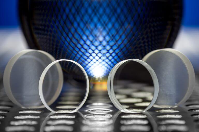
Fused Silica Wafer
Round Wafer – 2″ up to 400mm
Square Wafer 4×4 mm up to 400 x 400 mm
Thickness 100 µm up to 10000 µm
CMP Polished Ra<0,5 nm
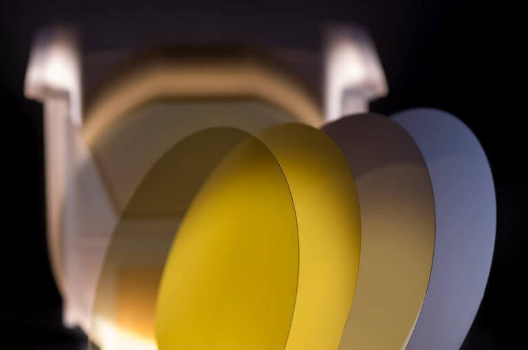
Glass Wafer
Round Wafer 5mm up to 400mm
Square Wafer 4×4 mm up to 10000 x 500 mm
Thickness 100 µm up to 10000 µm
CMP Polished Ra<0,5 nm

LT & LN Wafer
Optical & SAW- Grade
Round Wafer – 4″ up to 150mm
Square Wafer 10×10 mm up to 100 x 100 mm
Thickness 250 µm up to 1000 µm
Crystal Quartz Wafer
Optical & SAW- Grade
Round Wafer – 2″ up to 150mm
Square Wafer 10×10 mm up to 100 x 100 mm
Thickness 100 µm up to 4000 µm
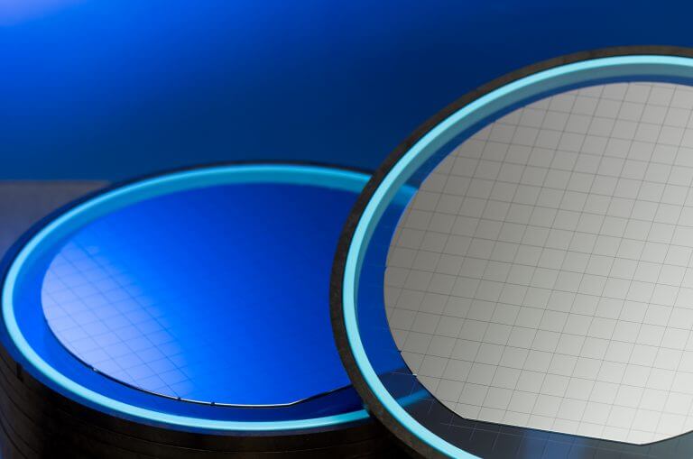
SOI & SI Wafer
SI Wafer – 2″ up to 300mm
SOI Wafer (SIMOX, SIMBOND) 6“ /8 „
SIC Wafer 4“/ 6“