About Us
Nano Quarz Wafer is a leading Supplier of high performance precision Optics and blank Wafers. Our goal is to become a reliable Partner for your Wafer Business, right from the Start with small Evaluation or Development Series up to a high volume Production in the Future. More than 20 years Experience in Wafer Technology and Production, helps us to produce, measure and deliver outstanding quality Solutions for a wide range of Industries.
As a business partner, Nano Quarz Wafer works with its Customers to design special Wafers that meet the exact Specifications and high Standards required in the Industries. Our core technical expertise includes Processing of Fused Silica, Glass, LT/LN Wafer, Quartz, Filters, a variety of low thermal expansion (CTE) materials and Silicon / SOI Wafer include reclaim for different materials.
Some Facts about NQW
Production
Our Production is based in Langenzenn, near Nuremberg/Germany. We uses state-of-the-art Equipment and Technologies to fulfill even the most demanding Specifications and Standards of our Customers.
- Manufacturing in a Clean Room Environment Class 4-6
- Integrated Management System with single Wafer Tracking and Tracing
Wafer Technology
Geometric features and the surface have a high importance for the Wafer-Quality. Special Parameters are used for the description of the surface, like GBIR, SFQR, Flatness, Roughness or Nanotopology. Global Geometry is described through Bow, WARP, Thickness, Thickness fluctuations (TTV).
Geometry / Surface
- Thickness: 100um up to 10mm
- Diameter: 2″ up to 300mm
- Bow < 20um
- Warp < 20 um
- TTV (GBIR) < 2 um
- LTV < 0,4 um (5x5mm2)
- SFQRmax (26x8mm, 90% PSA) < 0,5um
- Edge: C-Shape, Beveled, As Cut
- Semi Standard M001-1105 E
- Lasermarking (T7/OCR) SEMI M1
- Ra: <0,5 nm – AFM Measured (polished)
- Ra: 0,1 – 2,0 um (rough)
- DIN ISO 10110
Innovations
We are passionate about developing new technologies and process know-how. Together with our partners as well as in collaboration with renowned Universities we are researching the technologies of tomorrow.
Our target: to be one step ahead, in order to provide you with the highest quality of our products and services.
- Polyimid Film Removal of Glass Wafer – Reclaim Process
- 100um Thin Glass and Quartz Wafer available
- NQW developed CMP & Reclaim Process for Lithium tantalate wafer
- NQW developed a next level egde process with high accuracy.
- A new QR-Code-Systems improved the integrated management of NQW GmbH
- New substrates to meet the challenges of the OLED-production
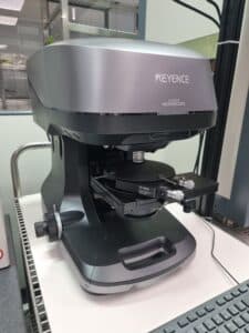
3D Laser Scanning Microscope
NanoQuarz Wafer GmbH is sending a strong signal for innovation and precision with the invest of the new 3D laser scanning microscope from KEYENCE. This
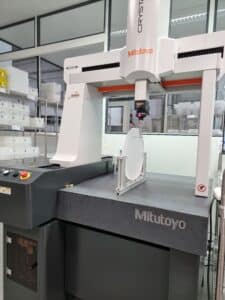
3D Coordinate Measuring Tool
With the invest in a modern 3D coordinate measuring machine from Mitutoyo, NanoQuarz Wafer GmbH is underlining its commitment to quality, efficiency, and innovation. This
Polyimid Film Removal of Glass Wafer – Reclaim Process
NQW developed a reclaim process for Glass wafer with multi-layer, structured Polyimid (PI) Films. The process is based on an organic alkaline chemical solutions and
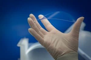
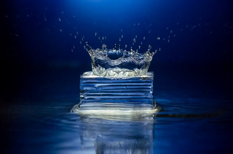
100um Thin Glass and Fused Silica Wafer available
NQW has developing a process to produce 100um Thin Borofloat33 and Fused Silica Wafer, and the transfer into production is successful completed. A special geometry
LT and LN wafer – New CMP & Reclaim Process
Lithium tantalate wafer in recent years, with the rapid development of communications, information industry development and industrialization of new optoelectronic materials. It has excellent piezoelectric
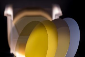
Substrate of glass for the field of organic electronics. (OLED)
NQW developed and supply for a leading provider of proprietary organic materials and additional innovative technologies for superior OLEDs in displays and lighting, the substrate