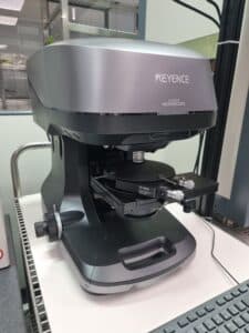
NanoQuarz Wafer GmbH is sending a strong signal for innovation and precision with the invest of the new 3D laser scanning microscope from KEYENCE. This investment underlines the company’s commitment to ensuring the highest quality standards.
The advantages at a glance:
Precision: Non-contact detection of wafer roughness with an accuracy of <0.5 nm enables detailed analysis of polished surfaces in the sub-nanometer range. With a resolution of Z:0.01 nm, XY: 0.1 nm, surface topography such as roughness, steps and geometric structures can be measured. The device offers three measurement methods, a confocal laser, focus variants and white light interferometry. This is crucial for ensuring the quality of the wafers.
Speed and efficiency: The microscope speeds up the analysis processes considerably, which leads to an optimization of production processes and a shorter time-to-market. This is particularly advantageous in an industry characterized by fast innovation cycles.
NanoQuarz Wafer GmbH can respond flexibly to the needs of its customers by using the broad applicability of the microscope in research, development, and production.The investment will improve internal processes and ensure that customers receive products of the highest quality.
Outlook:
Stay tuned for further updates and innovations from NanoQuarz Wafer GmbH. If you have any questions or require detailed information, please do not hesitate to contact the NanoQuarz Wafer GmbH team.