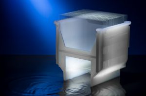
Organic light-emitting diode (OLED) displays are setting the bar higher and higher for the carrier substrates on which the organic layers have to be applied. This is especially true of glass substrates. Here, two market and technological trends compound the issue: rising demand for ever-larger terminal displays, and the trend towards installing both OLED technology and control electronics on the same substrates. For one thing, ensuring a smooth and even surface on larger glass displays requires a much more complex and exacting production and polishing process than with smaller substrate surfaces. Pairing the light-emitting components and controllers on one substrate is no easy task, either, but it allows for slimmer and more compact devices while maximising display size. SemiQuarz Wafer has identified the requirements these trends are creating for substrates, and developed the technologies to meet these challenges.
Geometric properties: hermiticity and roughness
Whether or not a glass substrate meets current industry requirements depends mainly on two criteria: the substrate’s geometry and the material it’s made from. Geometric requirements are primarily based on the substrate’s surface texture (hermiticity), with a differentiation between the local and the global perspective. The prime concern here is to obtain a homogenous nanotopography with a roughness of max. 10 nm at the local level, as any variations in substrate thickness can lead to unacceptable colour shifts, non-uniform luminance or even, in the worst case, to a short-circuit of individual pixels – all of which negatively impacts OLED longevity. From the global perspective, the global topography, measured in TTV (Total Thickness Variation), must be as even as possible because it will determine quality and performance of the applied OLEDs.
Substrate requirements
The second key criterion for determining the suitability of a specific substrate is the material it’s made from. The problem with most commercially available plastic substrates is their high air and moisture permeability, which may damage the cathode structure and impair OLED function. Studies conducted by Nano Quarz Wafer revealed OLED malfunctions when the substrate’s permeation rate exceeded 1 x 10⁻⁶ g/m² per day 25 degrees Celsius. In addition, the substrate must also meet specific requirements in terms of chemical resistance, temperature stability and moisture sensitivity.
SemiQuarz Wafer substrates have a solid track record
The products developed by Nano Quarz Wafer are the result of extensive research, development and testing – and they have already established themselves as the substrate of choice for OLED applications. With a total thickness variation of less than 2 micrometres and a roughness of less than .3 nanometres, they exceed the required quality standards by a multiple factor. To illustrate what these figures mean: the thickness variations on the surface of a substrate are on average just one 30th the thickness of a human hair; and.3 nm is equal to a third of a millionth of a millimetre (or about 30 angstroms or 10 atom layers), or a third of a ten-thousandth of the thickness of a human hair. SemiQuarz Wafer substrates are characterised by extremely high chemical purity and outstanding transmission behaviour across the spectrum from infrared to ultraviolet.
The knowledge and expertise that go into our solutions for the OLED market are just one example of the innovative drive at Nano Quarz Wafer. Our goal: to get customers and partners excited about the possibilities with high-quality, high-performance substrates for the most diverse applications.

